
Introduction:
For the past several decades, the exponential expansion of global digital infrastructure has relied on a foundational hardware medium: copper cabling. From internal motherboard traces and server rack backplanes to inter-rack data center switching fabrics, electrical signals transmitted across copper wires have served as the undisputed lifeblood of modern computing. We streamed high-definition video, deployed massive cloud databases, and trained complex artificial intelligence models by pushing electrons through copper conduits, trusting standard electrical engineering principles to sustain our growing bandwidth appetites.
Yet, this foundational reliance on copper interconnects faces a compounding, insurmountable physical bottleneck known in the semiconductor industry as the copper attenuation wall. As data center traffic scales exponentially—driven primarily by generative artificial intelligence workloads, hyperscale cloud computing, and real-time video streaming—servers must exchange petabytes of data per second.
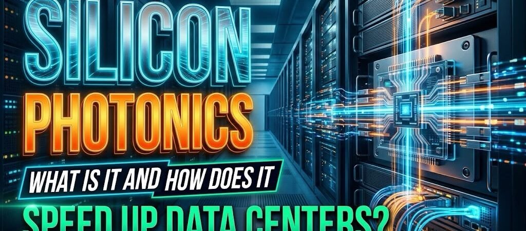
Enter silicon photonics—a revolutionary technological paradigm that replaces electrons with photons, integrating optical data transmission directly onto standard silicon semiconductor manufacturing lines. Promising multi-terabit bandwidths, near-zero latency, radical energy efficiency, and immunity to electromagnetic interference, silicon photonics represents the definitive architectural savior of modern hyperscale data centers. What is silicon photonics, how do optical integrated circuits manipulate light on silicon wafers, and how is photonics accelerating the future of cloud computing? In this comprehensive, exhaustive guide, we will deconstruct the physics of photonic integrated circuits (PICs), analyze co-packaged optics, explore AI cluster interconnect scaling, and evaluate whether optical networking is permanently replacing copper inside the data center.
1. Introduction to Optical Interconnects and the Copper Bottleneck in Hyperscale Data Centers
To understand why semiconductor fabricators and hyperscale cloud providers are aggressively pivoting toward silicon photonics, you must first examine the severe physical limitations governing electrical signal transmission over copper. In traditional data center architectures, servers inside racks communicate with top-of-rack switches via copper twinaxial cables, while switches communicate across rows via high-speed copper or legacy pluggable optical transceivers.
As data rates scale from 100 Gbps to 400 Gbps, 800 Gbps, and beyond 1.6 Terabits per second (Tbps) per port, copper conductors run hard against fundamental laws of physics described by Shannon’s theorem and transmission line theory. High-frequency electrical signals suffer from severe dielectric losses, meaning that as data frequency increases, the signal amplitude decays rapidly over distance. Consequently, high-speed electrical signals can travel only a few centimeters across a PCB motherboard trace or a couple of meters across a copper cable before becoming completely unintelligible due to noise and jitter.
2. Defining Silicon Photonics: Marrying Microelectronics with Integrated Optics
The term silicon photonics refers to the branch of photonics that studies and develops photonic systems which use silicon as an optical medium. Unlike traditional discrete optical components—which rely on bulk glass lenses, discrete laser diodes, and hand-aligned mirrors that are prohibitively expensive and difficult to scale—silicon photonics leverages the existing multi-billion-dollar manufacturing infrastructure of the semiconductor industry.
By utilizing standard Complementary Metal-Oxide-Semiconductor (CMOS) fabrication processes, engineers can etch microscopic optical waveguides, modulators, and photodetectors directly onto silicon wafers alongside electronic microprocessors and switch ASICs. This convergence marries the speed, bandwidth, and low-loss nature of light with the ultra-low cost, high precision, and mass-manufacturing scalability of silicon computer chips.
In a silicon photonic integrated circuit (PIC), laser light (typically generated at infrared wavelengths around 1,310 nm or 1,550 nm) is coupled into microscopic silicon waveguides etched directly onto the silicon die. These sub-micron waveguides guide photons around tight corners and through active optical components with extreme spatial precision, transforming a silicon chip into a sophisticated optical motherboard capable of routing terabits of data per second using light rather than electricity.
3. The Physics of Light vs. Electrons: Bandwidth, Attenuation, and Heat Dissipation
To fully appreciate the architectural superiority of silicon photonics over electrical copper interconnects, one must examine the fundamental physical differences between electrons and photons as carriers of digital information. Electrons possess mass and a negative electrical charge; when forced through a copper wire, they experience resistance (Joule heating), generate magnetic fields that cause crosstalk interference, and scatter against atomic lattice structures.
Photons, conversely, are massless packets of light operating at terahertz carrier frequencies. They possess no electrical charge, experience zero resistive electrical drop, and do not interact with neighboring light beams in free space or within properly designed waveguides. This fundamental divergence unlocks three decisive physical advantages for optical interconnects:
- Virtually Infinite Bandwidth Density: Optical carrier frequencies operate at hundreds of terahertz, enabling massive wavelength-division multiplexing where multiple distinct data streams travel down a single microscopic optical fiber simultaneously without mutual interference.
- Zero Distance-Dependent Attenuation: Where electrical signals degrade exponentially over meters of copper, optical photons travel across silicon waveguides and fiber-optic strands for kilometers with negligible signal loss.
- Thermal Elimination: Optical transmission generates virtually zero resistive heat dissipation within the interconnect path, slashing data center cooling requirements and eliminating thermal throttling bottlenecks.
For further academic insights into photonics physics and optical carrier wave mechanics, read research papers via Journal of Lightwave Technology Portal alongside advanced hardware evaluations at My Tech Hub Hardware News.
4. Complementary Metal-Oxide-Semiconductor (CMOS) Compatibility and Silicon Foundry Manufacturing
The single greatest economic and practical catalyst accelerating the rise of silicon photonics is its seamless compatibility with existing CMOS semiconductor manufacturing foundries. For decades, optical devices were manufactured using exotic compound semiconductor materials such as gallium arsenide (GaAs) or indium phosphide (InP). While these materials possess exceptional optical properties (such as the ability to emit laser light directly), they are extremely expensive, brittle, and restricted to low-volume specialty fabrication lines that cannot achieve the multi-million-unit economies of scale enjoyed by silicon chip foundries.
Silicon, however, is the foundational material of the global microelectronics industry. By adapting standard 300mm silicon wafer fabrication lines—the exact same cleanrooms utilized by TSMC, Intel, GlobalFoundries, and Samsung to manufacture advanced computer processors—foundries can manufacture millions of photonic integrated circuits with sub-nanometer precision using deep ultraviolet (DUV) and extreme ultraviolet (EUV) photolithography.
This CMOS compatibility means that optical modulators, photodetectors, and passive routing waveguides can be printed onto silicon wafers using automated, high-yield lithographic tools. By piggybacking on the trillion-dollar manufacturing capacity of the global silicon semiconductor ecosystem, silicon photonics achieves dramatic component cost reductions, paving the way for ubiquitous optical interconnect integration across mainstream enterprise hardware.
5. Optical Components on Silicon: Waveguides, Modulators, and Photodetectors
A fully functional silicon photonic integrated circuit (PIC) requires a complete suite of microscopic optical components to generate, route, modulate, and detect light signals. Because silicon is an indirect bandgap semiconductor, it cannot efficiently emit laser light on its own, but it excels at manipulating light once introduced onto the chip.
The core optical building blocks etched onto a silicon photonic die include:
- Silicon Waveguides: Microscopic channels of silicon surrounded by silicon dioxide (silica cladding) that trap and guide infrared light via total internal reflection, functioning like fiber-optic cables etched onto a flat chip surface.
- Optical Modulators: High-speed active components (typically utilizing the plasma dispersion effect in silicon pn-junctions) that rapidly alter the phase or intensity of light passing through the waveguide, translating electrical 1s and 0s into optical pulses.
- Photodetectors: Integrated germanium-on-silicon (Ge-on-Si) photodiodes that absorb incoming optical photons and convert them back into electrical current streams at the receiving end of the link.
By integrating these disparate optical components onto a single monolithic silicon die or multi-die co-packaged assembly, engineers create ultra-compact optical transceivers capable of multi-terabit bidirectional data exchange.
6. The Role of Silicon-On-Insulator (SOI) Substrates in Modern Photonic Integrated Circuits (PICs)
The manufacturing foundation of high-performance silicon photonics relies heavily on specialized semiconductor substrates known as Silicon-On-Insulator (SOI) wafers. A standard bulk silicon wafer is opaque and conducts light poorly across its entire thickness. To trap and guide light efficiently on a chip surface, engineers require a specialized sandwich structure.
An SOI wafer comprises three distinct vertical layers:
- A Thick Silicon Handle Substrate: The structural mechanical base of the wafer that provides physical rigidity during handling and fabrication.
- A Buried Oxide (BOX) Layer: A thick layer of silicon dioxide (typically 1 to 3 micrometers thick) that acts as an optical isolation barrier.
- A Thin Top Silicon Layer: A pristine, monocrystalline silicon film (ranging from 100 to 300 nanometers thick) in which optical waveguides and photonic structures are etched.
Because the refractive index of silicon (n \approx 3.48) is vastly higher than that of the underlying silicon dioxide insulator (n \approx 1.44), infrared light entering the top silicon layer is confined tightly within the waveguide via total internal reflection, preventing optical leakage into the substrate below. This high refractive index contrast allows engineers to construct ultra-compact optical bends and micro-resonators, shrinking optical circuits down to microscopic dimensions.
7. Laser Integration Challenges: Monolithic Growth vs. Hybrid and Heterogeneous Bonding
While silicon is an extraordinary medium for routing and modulating light, its physical crystal structure possesses an indirect bandgap, making it notoriously inefficient at emitting laser light when stimulated by electrical current. This fundamental limitation—the “silicon laser problem”—historically forced engineers to maintain separate, off-chip laser diodes manufactured from exotic III-V compound semiconductors (like indium phosphide).
Overcoming this physical hurdle has driven intense R&D investment into three primary laser integration methodologies:
- External Laser Coupling: Retaining separate laser packages off-chip and coupling light onto the silicon PIC via external polarization-maintaining fiber arrays. While reliable, this approach adds mechanical complexity and packaging costs.
- Hybrid and Heterogeneous Silicon Photonics: Bonding III-V semiconductor gain chips directly onto the surface of a silicon-on-insulator wafer using molecular bonding or adhesive polymers, allowing light from the III-V material to evanescently couple into the underlying silicon waveguides.
- Monolithic Epitaxial Growth: The long-term holy grail of growing III-V laser materials directly onto silicon crystal substrates during foundry manufacturing, though plagued by lattice mismatch defects.
Heterogeneous integration has emerged as the dominant commercial standard, enabling high-yield manufacturing of lasers integrated seamlessly onto silicon photonic wafers.
8. Co-Packaged Optics (CPO): Moving Optical Transceivers Closer to Switch ASICs
For years, enterprise data centers deployed pluggable optical transceivers—modular metal boxes plugged into the front faceplates of network switches. Inside these pluggable modules, electrical signals traveled across long PCB traces from the central switch ASIC to the transceiver edge, where they were converted into optical signals for transmission across fiber-optic cables.
However, as switch ASIC bandwidths surged to 51.2 Terabits and 102.4 Terabits per second, driving electrical signals across centimeters of motherboard copper traces from the ASIC to the front-panel pluggable modules became an unsustainable power sink, requiring excessive high-speed retimers and generating severe thermal bottlenecks.
The industry breakthrough solving this physical crisis is Co-Packaged Optics (CPO). In a CPO architecture, the traditional pluggable optical transceivers are eliminated entirely from the front bezel. Instead, silicon photonic optical engine dies are packaged directly onto the same multi-chip substrate or interposer right alongside the massive switch ASIC processor.
By placing the optical transceivers millimeters away from the processor cores, electrical traces are shortened drastically from tens of centimeters down to fractions of a millimeter. This eliminates high-frequency electrical loss, slashes power consumption by up to 50%, and enables unprecedented network switching bandwidth density. For further technical analyses on co-packaged optics architectures, explore documentation via IEEE Photonics Conference Portal or hardware reviews on My Tech Hub Hardware News.
9. Electrical vs. Optical Power Consumption: Slashing Data Center Energy Footprints
The staggering expansion of artificial intelligence, cloud computing, and hyperscale data centers has placed immense strain on global electrical grids. Modern AI training clusters consume megawatts of power continuously, with a significant fraction of that electricity dedicated entirely to thermal cooling and moving data between processors.
Evaluating the power consumption metrics between electrical copper interconnects and silicon photonics reveals a profound efficiency divergence:
- Copper Interconnects: Require heavy electrical amplification, serialization/deserialization (SerDes), and equalization circuits to overcome high-frequency attenuation, consuming roughly 15 to 25 picojoules per bit (pJ/bit) for rack-scale links.
- Silicon Photonics: Transmits photons across optical fibers with minimal loss, reducing optical transceiver power consumption down to 3 to 5 pJ/bit, while eliminating resistive line losses entirely.
This four-to-five-fold reduction in energy-per-bit transmission scales savings to the megawatt level across hyperscale data centers containing hundreds of thousands of servers. By slashing interconnect power dissipation, silicon photonics directly reduces data center operational expenditures and carbon footprints.
10. Eliminating Latency Bottlenecks in AI Cluster Training and Large Language Model (LLM) Scaling
The training of massive Large Language Models (LLMs) and foundation AI models relies on distributed cluster computing where thousands of specialized AI accelerators (GPUs and TPUs) cooperate simultaneously on a single training run. This distributed training process requires constant, massive parameter synchronization across processors via all-reduce and all-to-all collective communication operations.
If network latency spikes or bandwidth bottlenecks occur between even a fraction of the GPUs in an AI cluster, the entire cluster stalls, forcing expensive processing units to sit idle waiting for data packets to arrive—a devastating inefficiency known as GPU starvation.
Silicon photonics eliminates this latency bottleneck by delivering ultra-low latency, multi-terabit optical interconnect fabrics that link accelerators directly. Photons travel at the speed of light within optical fibers with zero electronic queuing delays, ensuring that gradient updates and model weights synchronize instantaneously across distributed server racks. This optical acceleration slashes LLM training times from months down to weeks, driving massive economic efficiencies for AI research labs.
11. Wavelength-Division Multiplexing (WDM) and Maximizing Fiber Optic Capacity
One of the most powerful engineering capabilities unlocked by silicon photonics is Wavelength-Division Multiplexing (WDM). In traditional electrical cabling, increasing bandwidth requires adding more physical copper wires or boosting signal frequencies, which exacerbates crosstalk and attenuation. In optical networking, WDM bypasses this physical limitation by multiplexing multiple distinct optical carrier wavelengths down a single microscopic strand of glass fiber.
Silicon photonic integrated circuits excel at micro-scale WDM integration. Using microscopic ring resonators and arrayed waveguide gratings (AWGs) etched directly onto the silicon die, engineers can combine dozens of distinct laser wavelengths—each modulated with independent multi-terabit data streams—onto a single optical fiber.
This multi-wavelength multiplexing multiplies fiber capacity exponentially without requiring the installation of new physical cable conduits. A single hair-thin optical fiber cable equipped with silicon photonic WDM transceivers can carry petabits of data per second, radically simplifying cable management and reducing spatial congestion beneath data center raised floors.
12. Optical Switching and Circuit-Switched Topologies for Hyperscale Networks
Traditional data center network topologies rely overwhelmingly on packet-switched electrical routers and switches. While packet switching is exceptional for handling unpredictable, bursty web traffic, it introduces routing overhead, buffering latency, and electronic processing bottlenecks when moving massive, sustained AI training datasets across hyperscale server clusters.
Silicon photonics enables the commercial realization of optical circuit switching (OCS). Instead of converting light back into electricity at every switching node to inspect packet headers, optical switches utilize micro-electromechanical systems (MEMS) or silicon Mach-Zehnder interferometer arrays to redirect beams of light physically from input ports to output ports at the speed of light.
This transparent, protocol-agnostic optical switching fabric allows hyperscale operators to reconfigure data center network topologies dynamically on the fly. When an AI cluster initiates a massive parameter transfer phase, the optical switch establishes a dedicated, zero-latency physical lightpath between GPU nodes, maximizing throughput and eliminating electrical queuing buffers.
13. Packaging, Thermal Management, and Optical-Electrical (O/E) Conversion Efficiency
While silicon photonics delivers breathtaking bandwidth and energy efficiencies, bringing optical integrated circuits out of the cleanroom and into commercial server racks introduces formidable mechanical and thermal packaging challenges. Photonic packaging is widely acknowledged as one of the most difficult engineering hurdles in modern semiconductor manufacturing.
Unlike traditional electronic chips that only require electrical wire bonds and plastic encapsulation, silicon photonic packages must accommodate:
- Optical Fiber Alignment: Coupling light from microscopic sub-micron silicon waveguides into hair-thin optical fibers with sub-micron alignment precision that must remain stable across thermal expansion cycles.
- Thermal Sensitivity: The refractive index of silicon is heavily dependent on temperature; a minor thermal shift inside a server rack can detune microscopic ring resonator filters, causing channel dropouts.
- Hermetic Sealing: Protecting sensitive laser facets and germanium photodetectors from atmospheric moisture and particulate contamination.
Solving these packaging complexities requires advanced automated robotic optical alignment, thermo-electric coolers (TECs) integrated onto multi-chip modules, and innovative edge-coupler designs that simplify fiber-to-chip optical attachment.
14. Testing, Metrology, and Automated Wafer-Level Optical Probing
In standard semiconductor manufacturing, electronic integrated circuits (ICs) are tested at the wafer level using automated probe cards equipped with thousands of tiny metal needles that touch electrical bond pads, verifying chip functionality in fractions of a second before packaging.
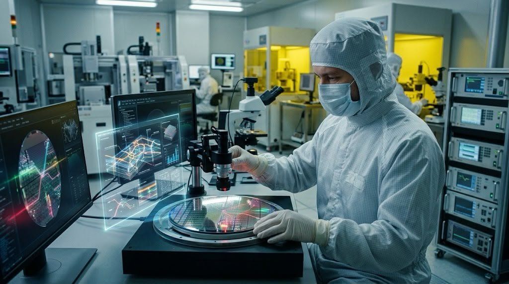
Testing silicon photonic integrated circuits introduces a profound metrology dilemma: you cannot test an optical chip with electrical needles alone. Because data travels via light, testing a photonic wafer requires coupling laser light into microscopic optical waveguides on the silicon die and measuring the exiting optical power using sensitive power meters.
Developing high-speed, automated wafer-level optical probing systems has required massive engineering innovation. Advanced metrology tools utilize robotic micro-positioners equipped with optical fiber arrays and vertical grating couplers to test thousands of photonic circuits per hour directly on the silicon wafer before dicing. This rigorous optical metrology ensures high manufacturing yields and prevents defective optical engines from entering expensive co-packaged modules.
15. Enterprise, Cloud Service Provider (CSP), and High-Performance Computing (HPC) Adoption Drivers
The commercial adoption of silicon photonics is driven by three powerful market segments with insatiable bandwidth appetites:
- Hyperscale Cloud Service Providers (CSPs): Companies like Microsoft, Amazon Web Services, Google, and Meta operate massive data centers housing hundreds of thousands of servers. Interconnecting these massive facilities requires millions of optical transceivers, making CSPs the primary financial engine driving volume adoption of silicon photonics to slash capital and operational expenditures.
- Artificial Intelligence (AI) Infrastructure Builders: Enterprises training trillion-parameter foundation models require ultra-low-latency accelerator fabrics, making silicon photonics and co-packaged optics non-negotiable for GPU cluster scalability.
- High-Performance Computing (HPC) & National Supercomputing Centers: Scientific research facilities simulating nuclear physics, climate modeling, and molecular chemistry demand multi-terabit interconnects that only photonics can deliver.
For further enterprise case studies and market adoption analyses, read reports via Hyperscale Cloud Infrastructure Research Desk alongside business strategy guides at My Tech Hub Business Portal.

16. Intellectual Property, Patent Landscapes, and Global Corporate Rivalries in Silicon Photonics
The rapid commercial maturation of silicon photonics, co-packaged optics, and optical transceiver integration has triggered an intense, multi-billion-dollar corporate race for global intellectual property dominance. Major semiconductor foundries, specialized silicon photonics startups, optical component manufacturers, and hyperscale cloud providers are fiercely patenting every conceivable breakthrough in heterogeneous laser bonding, sub-micron waveguide etching, automated optical packaging, and electro-optic modulators.
Securing foundational patents in this nascent industry dictates which corporations will control global supply chains, manufacturing licensing frameworks, and commercial distribution channels across the optical networking era. This high-stakes corporate rivalry has transformed advanced photonics university research laboratories and venture-backed spin-offs into prime acquisition targets.
Venture capital firms, sovereign wealth funds, and multinational tech giants are pouring massive capital injections into optical engineering teams capable of solving manufacturing yield hurdles. Furthermore, navigating global patent landscapes requires aggressive international legal strategies to prevent intellectual property infringement across competing jurisdictions. For comprehensive analyses on photonics patent filings and intellectual property trends in advanced optical hardware, explore reports via World Intellectual Property Organization (WIPO) Analytics Portal alongside market strategy guides at My Tech Hub Business Portal.
17. The Societal, Environmental, and Energy Sustainability Impact of Optical Data Centers
The widespread architectural transition toward silicon photonics and optical data centers introduces profound environmental, societal, and sustainability considerations. For decades, the explosive growth of internet traffic, video streaming, and cloud storage was accompanied by an alarming surge in global electrical energy consumption by data centers, drawing heavy criticism from environmental watchdogs regarding carbon emissions and grid strain.
The adoption of silicon photonics elevates optical networking from an optional high-performance corporate upgrade into an essential component of global energy sustainability. By slashing transceiver power consumption by up to 80% and eliminating high-frequency electrical line losses, silicon photonics directly curtails the massive electrical demand of hyperscale data centers.
Furthermore, lower power dissipation reduces thermal cooling loads, cutting water consumption required by industrial evaporative cooling towers. Aligning digital infrastructure expansion with rigorous global ecological climate mandates ensures that the artificial intelligence and cloud computing revolution does not compromise planetary energy sustainability.
18. Neurological and Algorithmic Analogies: Photonic Neural Networks and Optical Computing
Beyond simply moving data between electronic processors faster, advanced silicon photonics research is pushing into an even more radical frontier: optical computing and photonic neural networks. Because light beams can perform linear algebra operations (such as matrix multiplications) instantaneously via optical interference and diffraction as light passes through optical meshes, researchers are designing chips that compute using light rather than electrons.
In a photonic neural network, optical modulators and Mach-Zehnder interferometer meshes represent artificial neural network weights. When input data encoded as light intensities passes through the optical mesh, the matrix multiplication required for deep learning inference is executed at the speed of light with zero electronic latency and negligible energy consumption.
While still in experimental development stages compared to commercial silicon photonic interconnects, optical computing promises to shatter current von Neumann computing bottlenecks, unlocking ultra-low-power AI inference accelerators for edge and data center deployment.
19. Circular Economics, E-Waste Management, and Sustainable Silicon Photonics Manufacturing
As the global semiconductor manufacturing and data center hardware industry commits to aggressive carbon neutrality targets, evaluating the complete lifecycle environmental footprint of advanced optical networking equipment becomes paramount. While silicon photonic transceivers contribute positively to planetary sustainability by slashing operational energy consumption during their multi-year operational lifespan, questions inevitably arise regarding what happens to these advanced optical engines and packaging modules when servers reach the end of their operational usefulness.
To prevent future electronic waste and material pollution crises, sustainable manufacturing pioneers are heavily prioritizing circular economy principles. Leading silicon photonics foundries are designing modular product architectures featuring easily separable optical fiber arrays, recyclable aluminum heatsinks, and easily recoverable silicon and germanium sub-components.
These circular design methodologies ensure that when a data center switch or server blade undergoes eventual decommissioning, its optical and electronic components can be efficiently disassembled, recovered, and recycled back into raw manufacturing streams, preventing electronic waste accumulation.
20. The Ultimate Decision Framework: Evaluating Data Center Architecture Readiness for Silicon Photonics
As enterprise IT directors, data center facility architects, cloud infrastructure planners, and network engineers stand at this historic crossroads between legacy electrical copper interconnects and emerging silicon photonics, evaluating architectural readiness requires disciplined strategic planning. Rushing out to deploy bleeding-edge optical fabrics without analyzing thermal management infrastructure, optical transceiver compatibility, and capital expenditure budgets can lead to operational friction and misallocated investments.
To determine whether integrating silicon photonics makes financial and technical sense for your data center facility today, evaluate three core pillars: switch port bandwidth density, interconnect power consumption limits, and AI cluster scaling demands. If you manage high-density AI training clusters or hyperscale cloud fabrics where copper attenuation and electrical power limits throttle performance, deploying silicon photonics and co-packaged optics delivers immediate, transformative bandwidth and energy efficiency dividends. Evaluate your infrastructure blueprint, balance upfront capital investment against long-term power and speed savings, and decide whether your data center is ready to embrace the optical networking revolution.

Frequently Asked Questions (FAQ)
Q1: What is silicon photonics?
A: Silicon photonics is a technology that uses silicon as an optical medium to route, modulate, and process data using light (photons) rather than electricity (electrons), leveraging standard semiconductor manufacturing lines (CMOS foundries) to produce low-cost optical integrated circuits.
Q2: Why is silicon photonics needed in modern data centers?
A: Traditional copper cables suffer from severe attenuation, high-frequency signal loss, and extreme heat generation at high data rates (400 Gbps to 1.6+ Tbps). Silicon photonics eliminates these copper bottlenecks, providing multi-terabit bandwidth, ultra-low latency, and up to an 80% reduction in transceiver power consumption.
Q3: How does silicon photonics accelerate artificial intelligence (AI) training?
A: Training massive Large Language Models (LLMs) requires thousands of GPUs to synchronize parameters constantly. Silicon photonics provides ultra-low latency, high-bandwidth optical interconnect fabrics that eliminate GPU starvation, slashing model training times from months down to weeks.
Conclusion: Is Silicon Photonics the Definitive Future of Data Center Networking?
So, what is silicon photonics, and how does it speed up data centers? The definitive answer is yes, by replacing constrained electrical copper wires with high-speed optical photons integrated onto silicon chips, silicon photonics has solved the data center bandwidth and energy wall.
- The performance advantages are absolute. Silicon photonics delivers multi-terabit bandwidth density, distance-independent attenuation, near-zero latency, and massive energy savings that copper can never match.
- The future of cloud computing is optical. As co-packaged optics scale across hyperscale facilities and AI clusters, silicon photonics is cementing its role as the indispensable backbone of the modern digital economy.
Evaluate your data center infrastructure, your AI scaling roadmap, and your power consumption limits, and consider embracing the transformative power of silicon photonics for your network architecture.